- 您现在的位置:买卖IC网 > Sheet目录349 > PCA9624PW,118 (NXP Semiconductors)IC LED DRIVER RGBA 24-TSSOP
NXP Semiconductors
PCA9624
8-bit Fm+ I 2 C-bus 100 mA 40 V LED driver
[2]
[3]
[4]
[5]
[6]
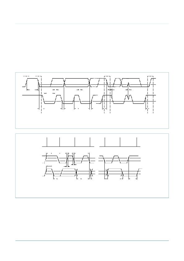
t VD;DAT = minimum time for SDA data out to be valid following SCL LOW.
A master device must internally provide a hold time of at least 300 ns for the SDA signal (refer to the V IL of the SCL signal) in order to
bridge the undefined region of SCL’s falling edge.
The maximum t f for the SDA and SCL bus lines is specified at 300 ns. The maximum fall time (t f ) for the SDA output stage is specified at
250 ns. This allows series protection resistors to be connected between the SDA and the SCL pins and the SDA/SCL bus lines without
exceeding the maximum specified t f .
C b = total capacitance of one bus line in pF.
Input filters on the SDA and SCL inputs suppress noise spikes less than 50 ns.
SDA
0.7 × V DD
0.3 × V DD
t BUF
t r
t f
t HD;STA
t SP
t LOW
SCL
0.7 × V DD
0.3 × V DD
t HD;STA
t SU;STA
t SU;STO
P
S
t HD;DAT
t HIGH
t SU;DAT
Sr
P
002aaa986
Fig 19. Definition of timing
protocol
START
condition
(S)
bit 7
MSB
(A7)
bit 6
(A6)
bit 1
(D1)
bit 0
(D0)
acknowledge
(A)
STOP
condition
(P)
SCL
t SU;STA
t LOW
t HIG H
1 / f SCL
0.7 × V DD
0.3 × V DD
SDA
t BUF
t r
t f
0.7 × V DD
0.3 × V DD
t HD;STA
t SU;DAT
t HD;DAT
t VD;DAT
t VD;ACK
t SU;STO
002aab285
Rise and fall times refer to V IL and V IH .
Fig 20. I 2 C-bus timing diagram
PCA9624
Product data sheet
All information provided in this document is subject to legal disclaimers.
Rev. 3 — 6 September 2012
? NXP B.V. 2012. All rights reserved.
27 of 37
发布紧急采购,3分钟左右您将得到回复。
相关PDF资料
PCA9625D/S911,518
IC LED DRIVER RGBA 32-SOIC
PCA9626BS,518
IC LED DRIVER RGBA 48HVQFN
PCA9632DP2,118
IC LED DRIVER RGBA 10-TSSOP
PCA9633BS,118
IC LED DRIVER RGBA 16-HVQFN
PCA9634D,118
IC LED DRIVER RGBA 20-SOIC
PCA9635PW/S911,118
IC LED DRIVER RGBA 28-TSSOP
PCA9685PW,118
IC LED DRIVER RGBA 28-TSSOP
PCA9922PW,118
IC LED DRIVER LINEAR 16-TSSOP
相关代理商/技术参数
PCA9624PW112
制造商:NXP Semiconductors 功能描述:IC LED DRVR TSSOP
PCA9625D
功能描述:LED照明驱动器 16BT I2C FMTP LED HVCON RST OE RoHS:否 制造商:STMicroelectronics 输入电压:11.5 V to 23 V 工作频率: 最大电源电流:1.7 mA 输出电流: 最大工作温度: 安装风格:SMD/SMT 封装 / 箱体:SO-16N
PCA9625D,512
功能描述:LED照明驱动器 16BT I2C FMTP LED HVCON RST OE RoHS:否 制造商:STMicroelectronics 输入电压:11.5 V to 23 V 工作频率: 最大电源电流:1.7 mA 输出电流: 最大工作温度: 安装风格:SMD/SMT 封装 / 箱体:SO-16N
PCA9625D,518
功能描述:LED照明驱动器 16-bit Fm I2C Bus 100mA 24 V LED drivr RoHS:否 制造商:STMicroelectronics 输入电压:11.5 V to 23 V 工作频率: 最大电源电流:1.7 mA 输出电流: 最大工作温度: 安装风格:SMD/SMT 封装 / 箱体:SO-16N
PCA9625D/S911,518
功能描述:LED照明驱动器 16BT I2C FMTP LED HVCON RST OE RoHS:否 制造商:STMicroelectronics 输入电压:11.5 V to 23 V 工作频率: 最大电源电流:1.7 mA 输出电流: 最大工作温度: 安装风格:SMD/SMT 封装 / 箱体:SO-16N
PCA9625D/S911-T
功能描述:LED照明驱动器 16BT I2C FMTP LED HVCON RST OE RoHS:否 制造商:STMicroelectronics 输入电压:11.5 V to 23 V 工作频率: 最大电源电流:1.7 mA 输出电流: 最大工作温度: 安装风格:SMD/SMT 封装 / 箱体:SO-16N
PCA9625DS911,518
功能描述:LED照明驱动器 16-bit Fm I2C Bus 100mA 24 V LED drivr RoHS:否 制造商:STMicroelectronics 输入电压:11.5 V to 23 V 工作频率: 最大电源电流:1.7 mA 输出电流: 最大工作温度: 安装风格:SMD/SMT 封装 / 箱体:SO-16N
PCA9625D-T
功能描述:LED照明驱动器 16BT I2C FMTP LED HVCON RST OE RoHS:否 制造商:STMicroelectronics 输入电压:11.5 V to 23 V 工作频率: 最大电源电流:1.7 mA 输出电流: 最大工作温度: 安装风格:SMD/SMT 封装 / 箱体:SO-16N
